COMPLEX TECHNOLOGY GRANTS SERVICES – OPPORTUNITY HIGHLIGHT: Semiconductor Packaging Research

Overview: On July 9, 2024, the Department of Commerce announced a new funding opportunity to support research and development (R&D) in semiconductor advanced packaging. This initiative, part of the CHIPS (Creating Helpful Incentives to Produce Semiconductors) for America program, aims to boost domestic capabilities in this field with up to $1.6B in funding.
Key Areas of Research: Funding will focus on five main R&D areas:
- Equipment and Processes: Developing new tools and methods for semiconductor packaging.
- Power and Heat Management: Improving how power is supplied and heat is managed in these systems.
- Connector Technology: Innovating in photonics and radio frequency (RF) connectors.
- Chiplets Ecosystem: Enhancing the ecosystem for small, modular chips.
- Co-Design and Automation: Creating better design tools for multi-chip systems.
There will also be opportunities for developing prototypes.
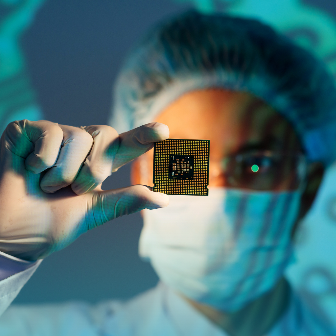
What is Advanced Packaging? Advanced packaging involves assembling multiple chips with different functions into a compact, multi-dimensional structure. This method significantly boosts performance and efficiency compared to traditional packaging on printed circuit boards. For instance, advancements in artificial intelligence rely heavily on this technology.
Why is This Important? Advanced packaging is crucial for U.S. manufacturers to remain competitive globally. However, it comes with several challenges, such as:
- Designing tightly integrated chips that function as a single unit.
- Managing power supply and heat dissipation.
- Testing and repairing complex assemblies.
- Ensuring reliability without traditional visual inspections.
Program Goals: The CHIPS National Advanced Packaging Manufacturing Program (NAPMP) aims to:
- Establish facilities to pilot new packaging technologies.
- Develop digital tools to streamline packaging engineering.
- Foster partnerships among industry, academia, and government to build a skilled workforce.
Priority Research Areas: The program will invest in six key areas:
- Materials and substrates.
- Equipment and processes.
- Power and thermal management.
- Photonics and connectors.
- Chiplet ecosystems.
- Co-design and automation tools.
For more detailed information, click on the full Notice of Intent (NOI): National Advanced Packaging Manufacturing Program | NIST
Navigating the grant process can be daunting, but you don’t have to do it alone. Lohfeld Consulting Group’s Grant Support Service is here to help you every step of the way, from identifying the right opportunities to crafting a winning proposal. Contact us today to learn how we can assist you in securing the funding your organization needs.
By Dana Katalinas, Vice President, APMP Member
Lohfeld Consulting Group has proven results specializing in helping companies create winning captures and proposals. As the premier capture and proposal services consulting firm focused exclusively on government markets, we provide expert assistance to government contractors in Capture Planning and Strategy, Proposal Management and Writing, Capture and Proposal Process and Infrastructure, and Training. In the last 3 years, we’ve supported over 550 proposals winning more than $170B for our clients—including the Top 10 government contractors. Lohfeld Consulting Group is your “go-to” capture and proposal source! Start winning by contacting us at www.lohfeldconsulting.com and join us on LinkedIn, Facebook, and YouTube(TM).
Paperback or Kindle
10 steps to creating high-scoring proposals
by Bob Lohfeld
contributors Edited by Beth Wingate
Subscribe to our free ebrief
Teaming friends, frenemies, and enemies—12 tips to mitigate harmful effects
Did you know that contracting officers spend up to 20% of their time mitigating disputes between teaming partners? In an informal poll we conducted on LinkedIn last month, 40% of respondents classified their teaming partners as “frenemies” on their last bid.
Explore Further
- Advice (543)
- AI (34)
- APMP (18)
- Army MAPS Contracts (7)
- Business Development (311)
- Capture Management (282)
- Complex Technology Grants Services (26)
- Favorite Books (5)
- GenAI (6)
- Go-to-Market (28)
- Graphics (5)
- Lohfeld Books (2)
- NASA SEWP VI Contracts (2)
- Navy SeaPort-NxG Contracts (2)
- NIST MSE Grants (1)
- NIST NAPMP Grants (2)
- Past Performance (64)
- Post-submission Phase (14)
- Pre-RFP Preparation (280)
- Proposal Management (357)
- Proposal Production (81)
- Proposal Reviews (50)
- Proposal Writing (119)
- Pursuit Phase (114)
- Research Report (4)
- Resources (64)
- Tools & Tips (446)
- Training (13)
- Uncategorized (223)

Sign Up for INSIGHTS and Download your FREE book
We'd love to help you with your proposals. Enjoy our complimentary Lohfeld Consulting Group Capture & Proposal Insights & Tips book with your FREE subscription to our Insights Newsletter.
GET YOUR FREE BOOK

